Congratulations On Your Successful Submission
 Submission Failure
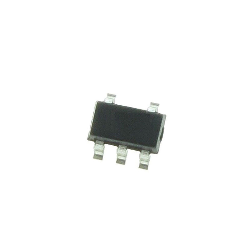
BU4S81G2
speed Logic Circuit
BU4S81G2
speed Logic Circuit
Quality Assurance
Quality Assurance
All parts procured from our supply chain network undergo a rigorous incoming inspection process. This meticulous inspection ensures that the parts received by our customers are authentic and meet the required standards. Additionally, we maintain detailed records of these inspections to ensure transparency and traceability throughout the supply chain.


Certification
We have successfully obtained various certification standards and have established our own professional testing laboratory. This ensures that every product we supply to our customers meets the highest quality standards. We adhere to strict testing protocols to maintain the consistency and accuracy of our products. To ensure that our products are original and genuine, we also collaborate with reputable third-party testing facilities to conduct rigorous quality testing. Our commitment to quality extends to meeting industry, legal, regulatory, and ISO 9001:2015 requirements.
Shipping & Payment
Shipping & Payment
About Shipping
We generally ship orders within a few business days through reliable shipping carriers such as FedEx, SF, UPS, or DHL. We also have support for other shipping methods. If you would like to inquire about specific shipping details or costs, please don't hesitate to reach out to us.


About Payment
We accept various payment methods, including VISA, MasterCard, UnionPay, Western Union, PayPal, and other channels.
If you have a specific payment method in mind or would like to inquire about rates and other details, please feel free to contact us.

WireTransfer

Paypal

CreditCard

WesternUnion

MoneyGram
Service & Packaging
Service & Packaging
About After Sales Service
All Parts Extended Quality Guarantee
Initiate the application within 90 days from the shipment date.
Confirm the return or exchange with our staff.
Maintain the goods in their original condition as received.
Lastly, please note that the eligibility for return or exchange of goods is subject to an assessment of the actual condition of the returned items. We will evaluate the received goods before finalizing the return or exchange process. If you have any inquiries or require further assistance regarding returns or exchanges, please don't hesitate to contact us at [email protected]
About packaging
Regarding packaging, our products are carefully packed in anti-static bags to provide ESD anti-static protection. The outer packaging is durable with secure closure. We support various packaging methods such as Tape and Reel, Cut Tape, Tube, or Tray.
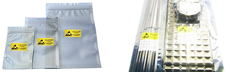
Example

Tape and Reel

Cut Tape

Tube or Tray
BU4S81G2 DataSheet

Current price plan is under preparation. Please contact our customer service team for the latest pricing information. Thank you for your understanding and support!
Details
General DescriptionThe BU4S11G2 is a 2-input NAND gate. An inverter-based buffer is incorporated at the gate output to improve I/O transmission characteristics, and it minimizes a variation in the propagation delay time caused by an increase in the load capacitance.Features■ Low power consumption■ High noise immunity■ Wide operating supply voltage range■ High input impedance■ High fan out■ Input can be directly driven 2 L-TTL inputs or 1 LS-TTL■ Buffered output
Key Features
- 1) Low power consumption
- 2) Surface mount package (SSOP5)
- 3) Broad operating supply voltage range: 3V-16V
- 4) High input impedance
- 5) High fan out
- 6) L-TTL2 and LS-TTL1 inputs can be driven directly.
- 7) Function compatible with BU4000B series (1ch).
Specifications
The followings are basic parameters of the part selected concerning the characteristics of the part and categories it belongs to.
| Pbfree Code | Yes | Rohs Code | Yes |
| Part Life Cycle Code | Active | Part Package Code | SSOP |
| Pin Count ! | 5 | Reach Compliance Code | compliant |
| HTS Code ! | 8542.39.00.01 | Family | 4000/14000/40000 |
| JESD-30 Code | R-PDSO-G5 | JESD-609 Code | e3 |
| Length | 2.9 mm | Load Capacitance (CL) | 50 pF |
| Logic IC Type | AND GATE | Moisture Sensitivity Level | 1 |
| Number of Functions | 1 | Number of Inputs | 2 |
| Number of Terminals | 5 | Operating Temperature-Max | 85 °C |
| Operating Temperature-Min | -40 °C | Package Body Material | PLASTIC/EPOXY |
| Package Code | LSSOP | Package Equivalence Code | TSOP5/6,.11,37 |
| Package Shape | RECTANGULAR | Package Style | SMALL OUTLINE, LOW PROFILE, SHRINK PITCH |
| Peak Reflow Temperature (Cel) | 260 | Power Supplies ! | 5/15 V |
| Propagation Delay (tpd) | 200 ns | Qualification Status ! | Not Qualified |
| Schmitt Trigger | NO | Seated Height-Max | 1.25 mm |
| Supply Voltage-Max (Vsup) | 16 V | Supply Voltage-Min (Vsup) | 3 V |
| Supply Voltage-Nom (Vsup) | 5 V | Surface Mount ! | YES |
| Technology | CMOS | Temperature Grade ! | INDUSTRIAL |
| Terminal Finish | TIN | Terminal Form ! | GULL WING |
| Terminal Pitch ! | 0.95 mm | Terminal Position | DUAL |
| Time@Peak Reflow Temperature-Max (s) | 10 | Width | 1.6 mm |
Datasheet PDF
Datasheets record the features, absolute maximum ratings, applications and more of the device, which benefit a lot as an overall guide to the specific application of the part.
FAQs
What is BU4S81G2?
The BU4S81G2 is a dual low-power CMOS logic gate IC manufactured by ROHM Semiconductor. It is designed for general digital logic applications where low power consumption and high-speed operation are essential.
How Does BU4S81G2 Work?
The BU4S81G2 functions as a dual 2-input AND gate, performing logical AND operations on two input signals to produce an output signal. It operates at low voltage levels and is suitable for battery-operated devices and portable electronics.
How Many Pins does BU4S81G2 have and What are the Functions of the Pinout Configuration?
The BU4S81G2 is typically available in a 8-pin SOP (Small Outline Package) configuration. The pinout configuration includes:
- 1A, 2A: Input pins for the first AND gate.
- 1B, 2B: Input pins for the second AND gate.
- 1Y, 2Y: Output pins for the respective AND gates.
- VCC: Positive power supply pin.
- GND: Ground pin.
What are the Pros and Cons of BU4S81G2?
Pros:
- Low Power Consumption: Ideal for low-power applications.
- High-Speed Operation: Enables rapid signal processing.
- Dual Functionality: Features two AND gates in a single package for space efficiency.
- Wide Operating Voltage Range: Suitable for various voltage levels.
Cons:
- Limited Functionality: Designed specifically for AND gate operations.
- Package Size: May require additional board space for larger SOP package.
Are There Any Equivalents/Alternatives to BU4S81G2 for Recommendation?
- The 74HC08 from Nexperia is an equivalent dual 2-input AND gate IC.
- Potential alternatives to the BU4S81G2 include the SN74LVC08A from Texas Instruments and the CD4081 from Texas Instruments.
Recommend Parts
-
![BA2901F]()
3,751 In Stock
Cargo cycle: 3~7 Days
The minimum order is 1
-
![BA4580RFVM]()
000uV Offset, Dual Function, PDSO8 Package, RoHS Certified
Brand: ROHM Package/Case: MSOP8
7,533 In Stock
Cargo cycle: 3~7 Days
The minimum order is 1