Congratulations On Your Successful Submission
 Submission Failure
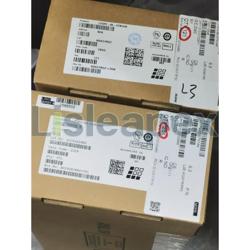
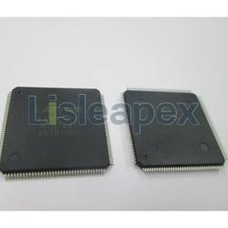
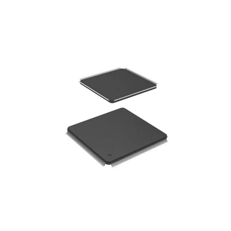
LFXP2-17E-5FTN256I
LatticeXP2 Family 17000 Cells 90nm Technology FPGA LFXP2-17E-5FTN256I 1.2V 256-Pin FTBGA Tray
LFXP2-17E-5FTN256I
LatticeXP2 Family 17000 Cells 90nm Technology FPGA LFXP2-17E-5FTN256I 1.2V 256-Pin FTBGA Tray
-
Manufacturer Part # : LFXP2-17E-5FTN256I
-
Package/Case: BGA
-
Brand: Lattice Semiconductor
-
Product Categories : FPGAs (Field Programmable Gate Array)
Quality Assurance
Quality Assurance
All parts procured from our supply chain network undergo a rigorous incoming inspection process. This meticulous inspection ensures that the parts received by our customers are authentic and meet the required standards. Additionally, we maintain detailed records of these inspections to ensure transparency and traceability throughout the supply chain.


Certification
We have successfully obtained various certification standards and have established our own professional testing laboratory. This ensures that every product we supply to our customers meets the highest quality standards. We adhere to strict testing protocols to maintain the consistency and accuracy of our products. To ensure that our products are original and genuine, we also collaborate with reputable third-party testing facilities to conduct rigorous quality testing. Our commitment to quality extends to meeting industry, legal, regulatory, and ISO 9001:2015 requirements.
Shipping & Payment
Shipping & Payment
About Shipping
We generally ship orders within a few business days through reliable shipping carriers such as FedEx, SF, UPS, or DHL. We also have support for other shipping methods. If you would like to inquire about specific shipping details or costs, please don't hesitate to reach out to us.


About Payment
We accept various payment methods, including VISA, MasterCard, UnionPay, Western Union, PayPal, and other channels.
If you have a specific payment method in mind or would like to inquire about rates and other details, please feel free to contact us.

WireTransfer

Paypal

CreditCard

WesternUnion

MoneyGram
Service & Packaging
Service & Packaging
About After Sales Service
All Parts Extended Quality Guarantee
Initiate the application within 90 days from the shipment date.
Confirm the return or exchange with our staff.
Maintain the goods in their original condition as received.
Lastly, please note that the eligibility for return or exchange of goods is subject to an assessment of the actual condition of the returned items. We will evaluate the received goods before finalizing the return or exchange process. If you have any inquiries or require further assistance regarding returns or exchanges, please don't hesitate to contact us at [email protected]
About packaging
Regarding packaging, our products are carefully packed in anti-static bags to provide ESD anti-static protection. The outer packaging is durable with secure closure. We support various packaging methods such as Tape and Reel, Cut Tape, Tube, or Tray.
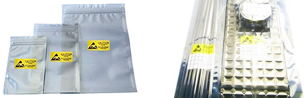
Example

Tape and Reel

Cut Tape

Tube or Tray
LFXP2-17E-5FTN256I DataSheet

Current price plan is under preparation. Please contact our customer service team for the latest pricing information. Thank you for your understanding and support!
Details
The LFXP2-17E-5FTN256I is a cutting-edge FPGA solution from Lattice Semiconductor, offering a unique combination of low power consumption, high performance, and flexibility. With its on-chip Flash-based In-System Programmability, this device allows for seamless reconfiguration in the field, ensuring adaptability for a wide range of applications. Boasting a logic capacity of 6,016 Look-Up Tables and 128 macrocells, the LFXP2-17E-5FTN256I is an ideal choice for small to medium-sized designs. Its 5 I/O banks and 56 I/O pins support various interface standards, making it versatile for different connectivity needs. Operating at a maximum frequency of 218 MHz and featuring a 256-pin FTN256 packaging, this FPGA is well-suited for space-constrained applications where high performance is essential. Its suitability for industrial control, communication, and consumer electronics applications further demonstrates its versatility and practicality, especially in scenarios where power efficiency is a critical consideration
Key Features
- Fully supports PowerPC™ 60x bus protocol, include PowerPC 603, 604, 740, 750 and 8260.
- Supports up to eight PowerPC bus masters with unlimited slave device support.
- Supports two outstanding bus accesses.
- Supports address only transfer and address bus retry.
- Independent address bus and data bus tenure with separate bus grant and data bus grant.
- Option for fixed priority assignment or rotating priority scheme.
- Designed for ASIC or programmable logic device implementations in various system environments.
- Fully static design with edge triggered flip-flops.
- Optimized for ispXPGA product family.

Specifications
The followings are basic parameters of the part selected concerning the characteristics of the part and categories it belongs to.
| Product Category ! | FPGA - Field Programmable Gate Array | RoHS | Details |
| Series | LFXP2 | Number of Logic Elements | 17000 LE |
| Adaptive Logic Modules - ALMs | 8500 ALM | Embedded Memory | 276 kbit |
| Number of I/Os | 201 I/O | Supply Voltage - Min | 1.14 V |
| Supply Voltage - Max | 1.26 V | Minimum Operating Temperature | - 40 C |
| Maximum Operating Temperature ! | + 100 C | Mounting Style | SMD/SMT |
| Package / Case | FTBGA-256 | Brand | Lattice |
| Distributed RAM | 35 kbit | Embedded Block RAM - EBR | 276 kbit |
| Height | 1.25 mm | Length | 17 mm |
| Maximum Operating Frequency | 311 MHz | Moisture Sensitive | Yes |
| Number of Logic Array Blocks - LABs | 2125 LAB | Operating Supply Voltage ! | 1.2 V |
| Product Type ! | FPGA - Field Programmable Gate Array | Factory Pack Quantity | 90 |
| Subcategory | Programmable Logic ICs | Total Memory | 311 kbit |
| Width | 17 mm | Unit Weight | 0.024868 oz |
Datasheet PDF
Datasheets record the features, absolute maximum ratings, applications and more of the device, which benefit a lot as an overall guide to the specific application of the part.
FAQs
What is LFXP2-17E-5FTN256I?
The LFXP2-17E-5FTN256I is a low-cost, low-power, and high-value field-programmable gate array (FPGA) designed by Lattice Semiconductor. It is ideal for applications requiring reconfigurable logic, such as industrial automation, communication systems, and consumer electronics.
How Does LFXP2-17E-5FTN256I Work?
The LFXP2-17E-5FTN256I works by enabling users to program the FPGA with custom logic functions to achieve specific application requirements. It features low power consumption, reconfigurable interconnects, and embedded block RAM, providing flexibility in implementing various digital functions.
How Many Pins does LFXP2-17E-5FTN256I have and What are the Functions of the Pinout Configuration?
The LFXP2-17E-5FTN256I is housed in a 256-pin fine pitch BGA (Ball Grid Array) package. The pinout configuration includes:
- IOBs (I/O Blocks): Used to connect external signals to the FPGA.
- PLL (Phase-Locked Loop): Provides clock generation and distribution for internal logic.
- Block RAM: Embedded memory blocks for data storage and retrieval.
- Configuration Pins: Used for device configuration and programming.
- Power and Ground Pins: Provide supply voltages and ground connections.
What are the Pros and Cons of LFXP2-17E-5FTN256I?
Pros:
- Low Power Consumption: Operates with low power, suitable for power-sensitive applications.
- Reconfigurability: Allows for on-the-fly reprogramming to adapt to changing requirements.
- Embedded Features: Includes embedded memory and PLL for enhanced functionality.
- Cost-Effective: Provides a low-cost solution for implementing custom logic functions.
- High I/O Density: Offers a high number of I/O pins for interfacing with external devices.
Cons:
- Complexity: Requires understanding of FPGA architecture and design tools for efficient utilization.
- Development Time: Designing and debugging FPGA logic can require significant development effort.
- Tool Dependency: Relies on vendor-specific development tools for programming and configuration.
Are There Any Equivalents/Alternatives to LFXP2-17E-5FTN256I for Recommendation?
- The Lattice LFXP2-5E from Lattice Semiconductor offers a smaller footprint with similar reconfigurable capabilities.
- Alternatives to the LFXP2-17E-5FTN256I include the Xilinx Spartan-7 series FPGAs and the Intel Cyclone series FPGAs.
Recommend Parts
-
![LFXP2-8E-5TN144I]()
8K LUT FPGA featuring 100 I/O instances designed for DSP tasks running at -5 speed grade and 1.2V
Brand: Lattice Package/Case: TQFP-144
6,343 In Stock
Cargo cycle: 3~7 Days
The minimum order is 1
-
![LFXP2-5E-5TN144I]()
Programmable Logic Device (CPLDs/FPGAs) 5000 625 TQFP-144(20x20)
Brand: Lattice Package/Case: TQFP-144
3,660 In Stock
Cargo cycle: 3~7 Days
The minimum order is 1
-
![LFXP2-40E-5FN484C]()
Versatile Field Programmable Gate Array operating at 435MHz frequency, featuring 40000 cells in a compact 23x23mm CMOS package
Brand: Lattice Package/Case: FPBGA-484
6,901 In Stock
Cargo cycle: 3~7 Days
The minimum order is 1
-
![LFXP2-5E-5TN144C]()
LFXP2-5E-5TN144C
$8.055 Field Programmable Gate Array
Brand: Lattice Semiconductor Package/Case: TQFP-144
4,219 In Stock
Cargo cycle: 3~7 Days
The minimum order is 1
-
![LFE3-35EA-8FN484C]()
LFE3-35EA-8FN484C
$11.045 LatticeECP3 Family FPGA with 484-Pin FBGA
Brand: Lattice Semiconductor Package/Case: BGA
5,860 In Stock
Cargo cycle: 3~7 Days
The minimum order is 1
-
![LFXP2-8E-5QN208C]()
7,685 In Stock
Cargo cycle: 3~7 Days
The minimum order is 1
-
![LFXP2-8E-5TN144C]()
7,718 In Stock
Cargo cycle: 3~7 Days
The minimum order is 1
-
![LFXP2-8E-5FTN256C]()
Advanced semiconductor technology
Brand: Lattice Semiconductor Package/Case: FTBGA-256
3,453 In Stock
Cargo cycle: 3~7 Days
The minimum order is 1
-
![LFXP2-17E-5FN484C]()
7,175 In Stock
Cargo cycle: 3~7 Days
The minimum order is 1
-
![LFXP2-5E-5QN208C]()
3,786 In Stock
Cargo cycle: 3~7 Days
The minimum order is 1
-
![LFE2-12E-5FN256C]()
7,498 In Stock
Cargo cycle: 3~7 Days
The minimum order is 1
-
![LFXP3C-3TN100C]()
3.1K LUTs and 62 I/O FPGA for Programmable Gate Array Applications
Brand: Lattice Semiconductor Package/Case: LQFP-100
4,452 In Stock
Cargo cycle: 3~7 Days
The minimum order is 1
-
![LFXP2-5E-6TN144C]()
LFXP2-5E-6TN144C
$9.304 5000 pieces of 625 TQFP-144(20x20) Programmable Logic Devices (CPLDs/FPGAs) meeting ROHS standards."
Brand: Lattice Semiconductor Package/Case: TQFP-144
6,318 In Stock
Cargo cycle: 3~7 Days
The minimum order is 1
-
![LFXP2-5E-5FTN256C]()
Field programmable gate array with 435MHz processing speed and 5000-cell capacity, in a CMOS PBGA256 package
Brand: Lattice Semiconductor Package/Case: BGA
3,124 In Stock
Cargo cycle: 3~7 Days
The minimum order is 1
-
![LFXP2-8E-5FTN256I]()
Programmable gate array with 8,000 look-up tables, 201 input/output interfaces, and dedicated digital signal processing unit operating at 1
Brand: Lattice Semiconductor Package/Case: BGA
4,301 In Stock
Cargo cycle: 3~7 Days
The minimum order is 1
-
![LCMXO3LF-9400C-5BG484C]()
LCMXO3LF-9400C-5BG484C
$9.484 Featuring 9400 logic elements and a 484-pin array
Brand: Lattice Semiconductor Package/Case: BGA
3,060 In Stock
Cargo cycle: 3~7 Days
The minimum order is 1