Congratulations On Your Successful Submission
 Submission Failure
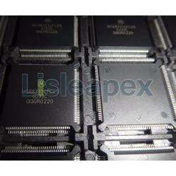
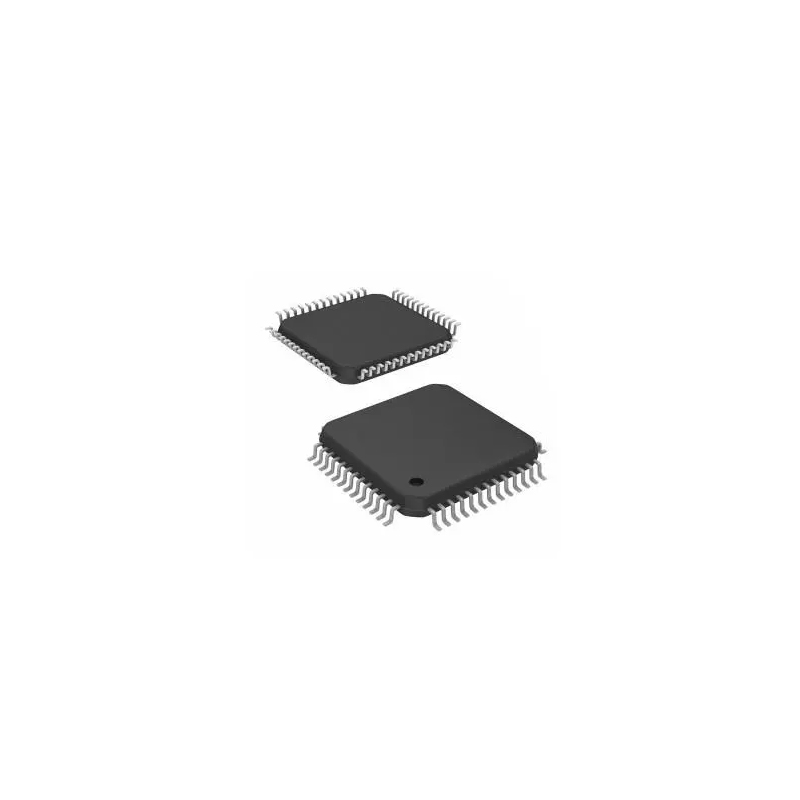
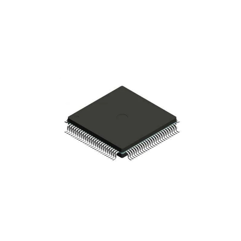
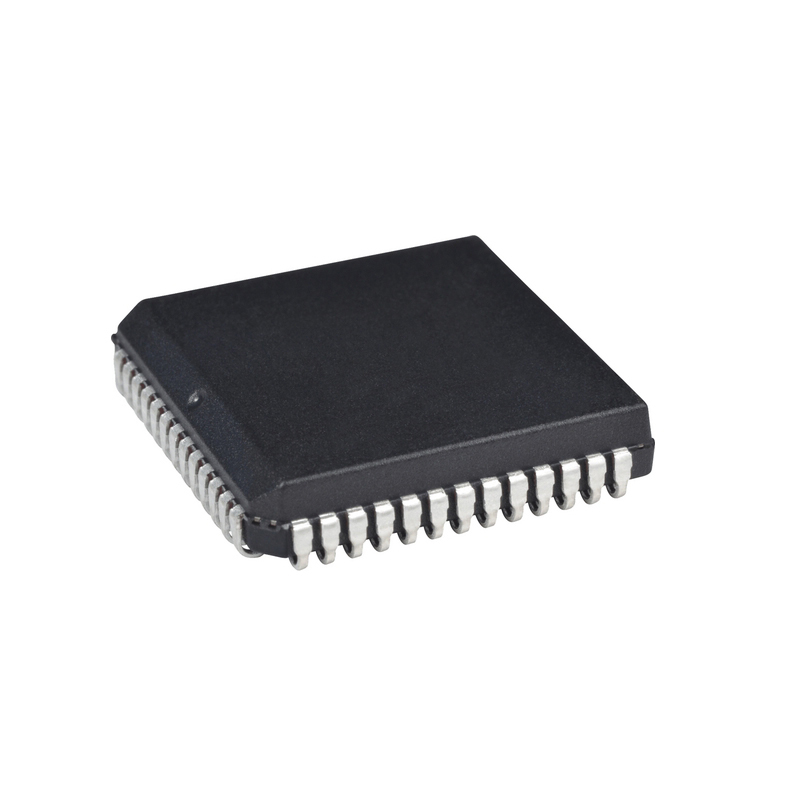
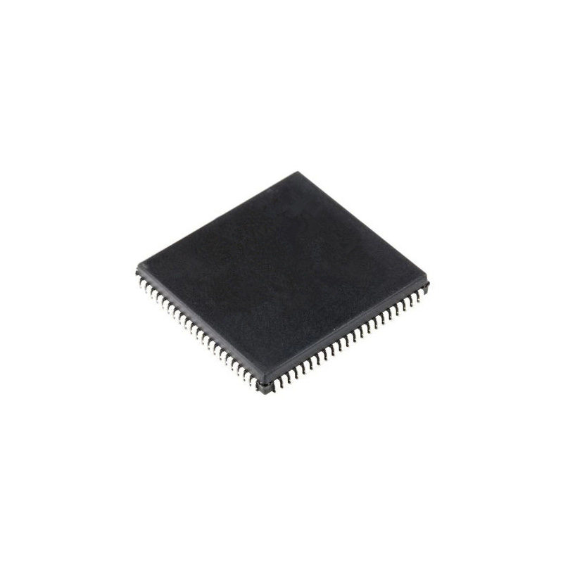
MC9S12E128CPV
25MHz processing speed
MC9S12E128CPV
25MHz processing speed
Quality Assurance
Quality Assurance
All parts procured from our supply chain network undergo a rigorous incoming inspection process. This meticulous inspection ensures that the parts received by our customers are authentic and meet the required standards. Additionally, we maintain detailed records of these inspections to ensure transparency and traceability throughout the supply chain.


Certification
We have successfully obtained various certification standards and have established our own professional testing laboratory. This ensures that every product we supply to our customers meets the highest quality standards. We adhere to strict testing protocols to maintain the consistency and accuracy of our products. To ensure that our products are original and genuine, we also collaborate with reputable third-party testing facilities to conduct rigorous quality testing. Our commitment to quality extends to meeting industry, legal, regulatory, and ISO 9001:2015 requirements.
Shipping & Payment
Shipping & Payment
About Shipping
We generally ship orders within a few business days through reliable shipping carriers such as FedEx, SF, UPS, or DHL. We also have support for other shipping methods. If you would like to inquire about specific shipping details or costs, please don't hesitate to reach out to us.


About Payment
We accept various payment methods, including VISA, MasterCard, UnionPay, Western Union, PayPal, and other channels.
If you have a specific payment method in mind or would like to inquire about rates and other details, please feel free to contact us.

WireTransfer

Paypal

CreditCard

WesternUnion

MoneyGram
Service & Packaging
Service & Packaging
About After Sales Service
All Parts Extended Quality Guarantee
Initiate the application within 90 days from the shipment date.
Confirm the return or exchange with our staff.
Maintain the goods in their original condition as received.
Lastly, please note that the eligibility for return or exchange of goods is subject to an assessment of the actual condition of the returned items. We will evaluate the received goods before finalizing the return or exchange process. If you have any inquiries or require further assistance regarding returns or exchanges, please don't hesitate to contact us at [email protected]
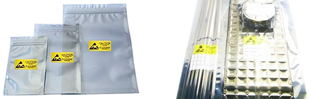
About packaging
Regarding packaging, our products are carefully packed in anti-static bags to provide ESD anti-static protection. The outer packaging is durable with secure closure. We support various packaging methods such as Tape and Reel, Cut Tape, Tube, or Tray.
Example

Tape and Reel

Cut Tape

Tube or Tray
MC9S12E128CPV DataSheet
Pricing (USD)
| Quantity | Unit Price | Ext. Price |
|---|---|---|
| 1 | $16.484 | $16.48 |
| 200 | $6.380 | $1,276.00 |
| 500 | $6.156 | $3,078.00 |
| 1000 | $6.045 | $6,045.00 |
These prices are subject to market fluctuations, and a quote submission is required to obtain the latest prices.
Details
IntroductionOverviewThe MC9S12E-Family is a 112/80 pin low cost general purpose MCU family. All members of the MC9S12E-Family are comprised of standard on-chip peripherals including a 16-bit central processing unit (HCS12 CPU), up to 256K bytes of Flash EEPROM, up to 16K bytes of RAM, three asynchronous serial communications interface modules (SCI), a serial peripheral interface (SPI), an Inter-IC Bus (IIC), three 4-channel 16-bit timer modules (TIM), a 6-channel 15-bit Pulse Modulator with Fault protection module (PMF), a 6-channel 8-bit Pulse Width Modulator (PWM), a 16-channel 10-bit analog-to-digital converter (ADC), and two 1-channel 8-bit digital-to-analog converters (DAC). The MC9S12E-Family has full 16-bit data paths throughout. The inclusion of a PLL circuit allows power consumption and performance to be adjusted to suit operational requirements. In addition to the I/O ports available on each module, 16 dedicated I/O port bits are available with Wake-Up capability from STOP or WAIT mode. Furthermore, an on chip bandgap based voltage regulator (VREG) generates the internal digital supply voltage of 2.5V (VDD) from a 3.135V to 5.5V external supply range.Features• 16-bit HCS12 CORE – HCS12 CPU i. Upward compatible with M68HC11 instruction set ii. Interrupt stacking and programmer’s model identical to M68HC11 iii. Instruction queue iv. Enhanced indexed addressing – Module Mapping Control (MMC) – Interrupt Control (INT) – Background Debug Module (BDM) – Debugger (DBG12) including breakpoints and change-of-flow trace buffer – Multiplexed External Bus Interface (MEBI)• Wake-Up interrupt inputs – Up to 16 port bits available for wake up interrupt function with digital filtering• Memory options – 32K, 64K, 128K or 256K Byte Flash EEPROM – 2K, 4K, 8K or 16K Byte RAM• Two 1-channel Digital-to-Analog Converters (DAC) – 8-bit resolution• Analog-to-Digital Converter (ADC) – 16-channel module with 10-bit resolution – External conversion trigger capability• Three 4-channel Timers (TIM) – Programmable input capture or output compare channels – Simple PWM mode – Counter Modulo Reset – External Event Counting – Gated Time Accumulation• 6 PWM channels (PWM) – Programmable period and duty cycle – 8-bit 6-channel or 16-bit 3-channel – Separate control for each pulse width and duty cycle – Center-aligned or left-aligned outputs – Programmable clock select logic with a wide range of frequencies – Fast emergency shutdown input• 6-channel Pulse width Modulator with Fault protection (PMF) – Three independent 15-bit counters with synchronous mode – Complementary channel operation – Edge and center aligned PWM signals – Programmable dead time insertion – Integral reload rates from 1 to 16 – Four fault protection shut down input pins – Three current sense input pins• Serial interfaces – Three asynchronous serial communication interfaces (SCI) – Synchronous serial peripheral interface (SPI) – Inter-IC Bus (IIC)• Clock and Reset Generator (CRG) – Windowed COP watchdog – Real Time interrupt – Clock Monitor – Pierce or low current Colpitts oscillator – Phase-locked loop clock frequency multiplier – Self Clock mode in absence of external clock – Low power 0.5 to 16Mhz crystal oscillator reference clock• Operating frequency – 50MHz equivalent to 25MHz Bus Speed• Internal 2.5V Regulator – Input voltage range from 3.135V to 5.5V – Low power mode capability – Includes low voltage reset (LVR) circuitry – Includes low voltage interrupt (LVI) circuitry• 112-Pin LQFP or 80-Pin QFP package – Up to 90 I/O lines with 5V input and drive capability (112 pin package) – Up to two dedicated 5V input only lines (IRQ and XIRQ) – Sixteen 3.3V/5V A/D converter inputs• Development Support. – Single-wire background debugTM mode – On-chip hardware breakpoints – Enhanced debug features
Key Features
- 16-bit HCS12 CORE
- — HCS12 CPU
- – i. Upward compatible with M68HC11 instruction set
- – ii. Interrupt stacking and programmer’s model identical to M68HC11
- – iii. Instruction queue
- – iv. Enhanced indexed addressing
- — Module Mapping Control (MMC)
- — Interrupt control (INT)
- — Background Debug Module (BDM)
- — Debugger (DBG12) including breakpoints and change-of-flow trace buffer
- — Multiplexed External Bus Interface (MEBI)
- Wake-Up interrupt inputs
- — Up to 16 port bits available for wake up interrupt function with digital filtering
- Memory Options
- — 32K, 64K or 128K Byte Flash EEPROM
- — 2K, 4K or 8K Byte RAM
- Two 1-channel Digital-to-Analog Converters (DAC)
- — 8-bit resolution
- Analog-to-Digital Converter (ADC)
- — 16-channel module with 10-bit resolution
- — External conversion trigger capability
- Three 4-channel Timers (TIM)
- — Programmable input capture or output compare channels
- — Simple PWM mode
- — Counter modulo reset
- — External event counting
- — Gated time accumulation
- 6 PWM channels (PWM)
- — Programmable period and duty cycle
- — 8-bit 6-channel or 16-bit 3-channel
- — Separate control for each pulse width and duty cycle
- — Center-aligned or left-aligned outputs
- — Programmable clock select logic with a wide range of frequencies
- — Fast emergency shutdown input
- 6-channel Pulse width Modulator with Fault protection (PMF)
- — Three independent 15-bit counters with synchronous mode
- — Complementary channel operation
- — Edge and center aligned PWM signals
- — Programmable dead time insertion
- — Integral reload rates from 1 to 16
- — Four fault protection shut down input pins
- — Three current sense input pins
- Serial interfaces
- — Three asynchronous serial communication interfaces (SCI)
- — Synchronous serial peripheral interface (SPI)
- — Inter-IC Bus (IIC)
- Clock and Reset Generator (CRG)
- — Windowed COP watchdog
- — Real Time interrupt
- — Clock Monitor
- — Pierce or low current Colpitts oscillator
- — Phase-locked loop clock frequency multiplier
- — Self Clock mode in absence of external clock
- — Low power 0.5 to 16Mhz crystal oscillator reference clock
- Operating frequency
- — 50MHz equivalent to 25MHz Bus Speed
- Internal 2.5V Regulator
- — Input voltage range from 3.135V to 5.5V
- — Low power mode capability
- — Includes low voltage reset (LVR) circuitry
- — Includes low voltage interrupt (LVI) circuitry
- 112-Pin LQFP or 80-Pin QFP or 64-Pin QFN package
- — Up to 90 I/O lines with 5V input and drive capability (112 pin package)
- — Up to two dedicated 5V input only lines (IRQ and XIRQ)
- — Sixteen 3.3V/5V A/D converter inputs
- Development Support.
- — Single-wire background debugTM mode
- — On-chip hardware breakpoints
- — Enhanced debug features
Specifications
The followings are basic parameters of the part selected concerning the characteristics of the part and categories it belongs to.
| Part Life Cycle Code | Active | Part Package Code | QFP |
| Pin Count ! | 112 | Reach Compliance Code | |
| Has ADC | YES | Address Bus Width ! | 16 |
| Bit Size | 16 | Clock Frequency-Max | 16 MHz |
| DAC Channels | YES | DMA Channels | NO |
| External Data Bus Width | 16 | JESD-30 Code | S-PQFP-G112 |
| Length | 20 mm | Number of I/O Lines | 92 |
| Number of Terminals | 112 | Operating Temperature-Max | 85 °C |
| Operating Temperature-Min | -40 °C | PWM Channels | YES |
| Package Body Material | PLASTIC/EPOXY | Package Code | LQFP |
| Package Shape | SQUARE | Package Style | FLATPACK, LOW PROFILE |
| ROM Programmability | FLASH | Seated Height-Max | 1.6 mm |
| Speed | 25 MHz | Supply Voltage-Max | 2.75 V |
| Supply Voltage-Min | 2.35 V | Supply Voltage-Nom | 2.5 V |
| Surface Mount ! | YES | Technology | CMOS |
| Temperature Grade ! | INDUSTRIAL | Terminal Form ! | GULL WING |
| Terminal Pitch ! | 0.65 mm | Terminal Position | QUAD |
| Width | 20 mm | uPs/uCs/Peripheral ICs Type | MICROCONTROLLER |
Datasheet PDF
Datasheets record the features, absolute maximum ratings, applications and more of the device, which benefit a lot as an overall guide to the specific application of the part.
Recommend Parts
-
![MC68HC11F1VFN4]()
5,008 In Stock
Cargo cycle: 3~7 Days
The minimum order is 1
-
![MC68HC16Z1CFC16]()
Plastic Quad Flat Pack (PQFP)132 Housing
Brand: Freescale Semiconductor Package/Case: PQFP-132
5,491 In Stock
Cargo cycle: 3~7 Days
The minimum order is 1
-
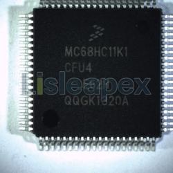
![MC68HC11K1CFU4]()
MC68HC11K1CFU4: High-Speed HCMOS Microcontroller
Brand: FREESCALE Package/Case: QFP80
4,132 In Stock
Cargo cycle: 3~7 Days
The minimum order is 1
-
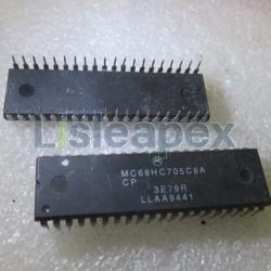
![MC68HC705C8ACP]()
5,768 In Stock
Cargo cycle: 3~7 Days
The minimum order is 1
-
![MC68331CFC25]()
MC68331CFC25 is a 32-bit microcontroller with 132 pins in PQFP package
Brand: FREESCALE Package/Case: DC9913 PACKAGE QFP132PIN
3,162 In Stock
Cargo cycle: 3~7 Days
The minimum order is 1
-
![MC68332CFC16]()
Microcontroller with 32-bit architecture, 16.78MHz clock speed, and 68000 CPU
Brand: FREESCALE Package/Case: QFP152
7,752 In Stock
Cargo cycle: 3~7 Days
The minimum order is 1
-
![MC9S12H128VFV]()
High-performance 16-bit flash microcontroller with 16MHz speed and pins in PQFP144 and LQFP-144 packages
Brand: FREESCALE Package/Case: TQFP-144
7,029 In Stock
Cargo cycle: 3~7 Days
The minimum order is 1
-
![MC68HC908AZ60AVFU]()
5,827 In Stock
Cargo cycle: 3~7 Days
The minimum order is 1
-
![MCF51CN128]()
High-speed microcontroller with flash memory operating at 50.33MHz, in a PQFP-80 package
Brand: FREESCALE Package/Case: QFN
4,886 In Stock
Cargo cycle: 3~7 Days
The minimum order is 1
-
![MC68HC705B16NCFNE]()
3,050 In Stock
Cargo cycle: 3~7 Days
The minimum order is 1
-
![MC68HC711K4]()
Highly programmable device for a wide range of applications
Brand: FREESCALE Package/Case: PLCC84
7,526 In Stock
Cargo cycle: 3~7 Days
The minimum order is 1
-
![MC9RS08KA1]()
MC9RS08KA1 is a 8-bit microcontroller with 4KB flash and 256B RAM, ideal for small embedded applications.
Brand: FREESCALE Package/Case: SOP8
3,004 In Stock
Cargo cycle: 3~7 Days
The minimum order is 1
-
![MC908QY4AC]()
6,906 In Stock
Cargo cycle: 3~7 Days
The minimum order is 1
-
![DSP56F807PY80]()
Ideal for applications requiring high performance and flash storage
Brand: Freescale Semiconductor Package/Case: LQFP-160
6,637 In Stock
Cargo cycle: 3~7 Days
The minimum order is 1
-
![DSPC56371AF180]()
6,012 In Stock
Cargo cycle: 3~7 Days
The minimum order is 1