Congratulations On Your Successful Submission
 Submission Failure
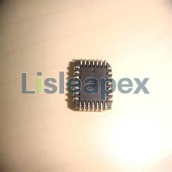
XPC855TZP50D4
Microprocessors - MPU XPC855TZP50D4XPC855TZP50D4
Microprocessors - MPU XPC855TZP50D4
Quality Assurance
Quality Assurance
All parts procured from our supply chain network undergo a rigorous incoming inspection process. This meticulous inspection ensures that the parts received by our customers are authentic and meet the required standards. Additionally, we maintain detailed records of these inspections to ensure transparency and traceability throughout the supply chain.


Certification
We have successfully obtained various certification standards and have established our own professional testing laboratory. This ensures that every product we supply to our customers meets the highest quality standards. We adhere to strict testing protocols to maintain the consistency and accuracy of our products. To ensure that our products are original and genuine, we also collaborate with reputable third-party testing facilities to conduct rigorous quality testing. Our commitment to quality extends to meeting industry, legal, regulatory, and ISO 9001:2015 requirements.
Shipping & Payment
Shipping & Payment
About Shipping
We generally ship orders within a few business days through reliable shipping carriers such as FedEx, SF, UPS, or DHL. We also have support for other shipping methods. If you would like to inquire about specific shipping details or costs, please don't hesitate to reach out to us.


About Payment
We accept various payment methods, including VISA, MasterCard, UnionPay, Western Union, PayPal, and other channels.
If you have a specific payment method in mind or would like to inquire about rates and other details, please feel free to contact us.

WireTransfer

Paypal

CreditCard

WesternUnion

MoneyGram
Service & Packaging
Service & Packaging
About After Sales Service
All Parts Extended Quality Guarantee
Initiate the application within 90 days from the shipment date.
Confirm the return or exchange with our staff.
Maintain the goods in their original condition as received.
Lastly, please note that the eligibility for return or exchange of goods is subject to an assessment of the actual condition of the returned items. We will evaluate the received goods before finalizing the return or exchange process. If you have any inquiries or require further assistance regarding returns or exchanges, please don't hesitate to contact us at [email protected]
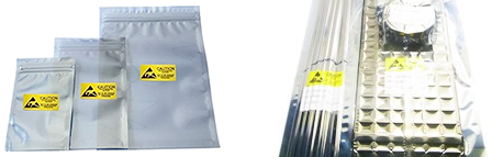
About packaging
Regarding packaging, our products are carefully packed in anti-static bags to provide ESD anti-static protection. The outer packaging is durable with secure closure. We support various packaging methods such as Tape and Reel, Cut Tape, Tube, or Tray.
Example

Tape and Reel

Cut Tape

Tube or Tray
XPC855TZP50D4 DataSheet

Current price plan is under preparation. Please contact our customer service team for the latest pricing information. Thank you for your understanding and support!
Details
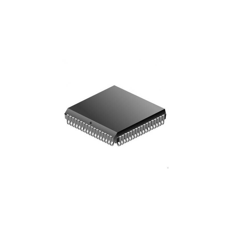
Overview The MPC860 Quad Integrated Communications Controller (PowerQUICC™) is a versatile one-chip integrated microprocessor and peripheral combination designed for a variety of controller applications. It particularly excels in both communications and networking systems. The PowerQUICC unit is referred to as the MPC860 in this manual.Features The following list summarizes the key MPC860 features: • Embedded single-issue, 32-bit MPC8xx core (implementing the PowerPC architecture) with thirty-two 32-bit general-purpose registers (GPRs) — The core performs branch prediction with conditional prefetch, without conditional execution — 4- or 8-Kbyte data cache and 4- or 16-Kbyte instruction cache (see Table 1) – 16-Kbyte instruction caches are four-way, set-associative with 256 sets; 4-Kbyte instruction caches are two-way, set-associative with 128 sets. – 8-Kbyte data caches are two-way, set-associative with 256 sets; 4-Kbyte data caches are two-way, set-associative with 128 sets. – Cache coherency for both instruction and data caches is maintained on 128-bit (4-word) cache blocks. – Caches are physically addressed, implement a least recently used (LRU) replacement algorithm, and are lockable on a cache block basis. — Instruction and data caches are two-way, set-associative, physically addressed, LRU replacement, and lockable on-line granularity. — MMUs with 32-entry TLB, fully associative instruction, and data TLBs — MMUs support multiple page sizes of 4, 16, and 512 Kbytes, and 8 Mbytes; 16 virtual address spaces and 16 protection groups — Advanced on-chip-emulation debug mode • Up to 32-bit data bus (dynamic bus sizing for 8, 16, and 32 bits) • 32 address lines • Operates at up to 80 MHz • Memory controller (eight banks) — Contains complete dynamic RAM (DRAM) controller — Each bank can be a chip select or RASto support a DRAM bank — Up to 15 wait states programmable per memory bank — Glueless interface to DRAM, SIMMS, SRAM, EPROM, Flash EPROM, and other memory devices. — DRAM controller programmable to support most size and speed memory interfaces — Four CASlines, four WElines, one OEline — Boot chip-select available at reset (options for 8-, 16-, or 32-bit memory) — Variable block sizes (32 Kbyte to 256 Mbyte) — Selectable write protection — On-chip bus arbitration logic • General-purpose timers — Four 16-bit timers or two 32-bit timers — Gate mode can enable/disable counting — Interrupt can be masked on reference match and event capture • System integration unit (SIU) — Bus monitor — Software watchdog — Periodic interrupt timer (PIT) — Low-power stop mode — Clock synthesizer — Three parallel I/O registers with open-drain capability • Four baud-rate generators (BRGs) — Independent (can be connected to any SCC or SMC) — Allow changes during operation — Autobaud support option • Four serial communications controllers (SCCs) — Ethernet/IEEE 802.3 optional on SCC1–4, supporting full 10-Mbps operation (available only on specially programmed devices). — HDLC/SDLC(all channels supported at 2 Mbps) — HDLC bus (implements an HDLC-based local area network (LAN)) — Asynchronous HDLC to support PPP (point-to-point protocol) — AppleTalk — Universal asynchronous receiver transmitter (UART) — Synchronous UART — Serial infrared (IrDA) — Binary synchronous communication (BISYNC) — Totally transparent (bit streams) — Totally transparent (frame based with optional cyclic redundancy check (CRC)) • Two SMCs (serial management channels) — UART — Transparent — General circuit interface (GCI) controller — Can be connected to the time-division multiplexed (TDM) channels • One SPI (serial peripheral interface) — Supports master and slave modes — Supports multimaster operation on the same bus • One I2C (inter-integrated circuit) port — Supports master and slave modes — Multiple-master environment support • Time-slot assigner (TSA) — Allows SCCs and SMCs to run in multiplexed and/or non-multiplexed operation — Supports T1, CEPT, PCM highway, ISDN basic rate, ISDN primary rate, user defined — 1- or 8-bit resolution — Allows independent transmit and receive routing, frame synchronization, clocking — Allows dynamic changes — Can be internally connected to six serial channels (four SCCs and two SMCs) • Parallel interface port (PIP) — Centronics interface support — Supports fast connection between compatible ports on the MPC860 or the MC68360 • PCMCIA interface — Master (socket) interface, release 2.1 compliant — Supports two independent PCMCIA sockets — Eight memory or I/O windows supported • Low power support — Full on—all units fully powered — Doze—core functional units disabled, except time base decrementer, PLL, memory controller, RTC, and CPM in low-power standby — Sleep—all units disabled, except RTC and PIT, PLL active for fast wake up — Deep sleep—all units disabled including PLL, except RTC and PIT — Power down mode— all units powered down, except PLL, RTC, PIT, time base, and decrementer • Debug interface — Eight comparators: four operate on instruction address, two operate on data address, and two operate on data — Supports conditions: =≠<> — Each watchpoint can generate a break-point internally • 3.3 V operation with 5-V TTL compatibility except EXTAL and EXTCLK • 357-pin ball grid array (BGA) package

Key Features
- The following list summarizes the key MPC860 features:
- Embedded single-issue, 32-bit MPC8xx core (implementing the PowerPC architecture) with thirty-two 32-bit general-purpose registers (GPRs)
- — The core performs branch prediction with conditional prefetch, without conditional execution
- — 4- or 8-Kbyte data cache and 4- or 16-Kbyte instruction cache (see Table 1)
- – 16-Kbyte instruction caches are four-way, set-associative with 256 sets;
- 4-Kbyte instruction caches are two-way, set-associative with 128 sets.
- – 8-Kbyte data caches are two-way, set-associative with 256 sets; 4-Kbyte data caches are two-way, set-associative with 128 sets.
- – Cache coherency for both instruction and data caches is maintained on 128-bit (4-word) cache blocks.
- – Caches are physically addressed, implement a least recently used (LRU) replacement algorithm, and are lockable on a cache block basis.
- — Instruction and data caches are two-way, set-associative, physically addressed, LRU replacement, and lockable on-line granularity.
- — MMUs with 32-entry TLB, fully associative instruction, and data TLBs
- — MMUs support multiple page sizes of 4, 16, and 512 Kbytes, and 8 Mbytes; 16 virtual address spaces and 16 protection groups
- — Advanced on-chip-emulation debug mode
- Up to 32-bit data bus (dynamic bus sizing for 8, 16, and 32 bits)
- 32 address lines
- Operates at up to 80 MHz
- Memory controller (eight banks)
- — Contains complete dynamic RAM (DRAM) controller
- — Each bank can be a chip select or RASto support a DRAM bank
- — Up to 15 wait states programmable per memory bank
- — Glueless interface to DRAM, SIMMS, SRAM, EPROM, Flash EPROM, and other memory devices.
- — DRAM controller programmable to support most size and speed memory interfaces
- — Four CASlines, four WElines, one OEline
- — Boot chip-select available at reset (options for 8-, 16-, or 32-bit memory)
- — Variable block sizes (32 Kbyte to 256 Mbyte)
- — Selectable write protection
- — On-chip bus arbitration logic
- General-purpose timers
- — Four 16-bit timers or two 32-bit timers
- — Gate mode can enable/disable counting
- — Interrupt can be masked on reference match and event capture
- System integration unit (SIU)
- — Bus monitor
- — Software watchdog
- — Periodic interrupt timer (PIT)
- — Low-power stop mode
- — Clock synthesizer
- — Three parallel I/O registers with open-drain capability
- Four baud-rate generators (BRGs)
- — Independent (can be connected to any SCC or SMC)
- — Allow changes during operation
- — Autobaud support option
- Four serial communications controllers (SCCs)
- — Ethernet/IEEE 802.3 optional on SCC1–4, supporting full 10-Mbps operation (available only on specially programmed devices).
- — HDLC/SDLC(all channels supported at 2 Mbps)
- — HDLC bus (implements an HDLC-based local area network (LAN))
- — Asynchronous HDLC to support PPP (point-to-point protocol)
- — AppleTalk
- — Universal asynchronous receiver transmitter (UART)
- — Synchronous UART
- — Serial infrared (IrDA)
- — Binary synchronous communication (BISYNC)
- — Totally transparent (bit streams)
- — Totally transparent (frame based with optional cyclic redundancy check (CRC))
- Two SMCs (serial management channels)
- — UART
- — Transparent
- — General circuit interface (GCI) controller
- — Can be connected to the time-division multiplexed (TDM) channels
- One SPI (serial peripheral interface)
- — Supports master and slave modes
- — Supports multimaster operation on the same bus
- One I2C (inter-integrated circuit) port
- — Supports master and slave modes
- — Multiple-master environment support
- Time-slot assigner (TSA)
- — Allows SCCs and SMCs to run in multiplexed and/or non-multiplexed operation
- — Supports T1, CEPT, PCM highway, ISDN basic rate, ISDN primary rate, user defined
- — 1- or 8-bit resolution
- — Allows independent transmit and receive routing, frame synchronization, clocking
- — Allows dynamic changes
- — Can be internally connected to six serial channels (four SCCs and two SMCs)
- Parallel interface port (PIP)
- — Centronics interface support
- — Supports fast connection between compatible ports on the MPC860 or the MC68360
- PCMCIA interface
- — Master (socket) interface, release 2.1 compliant
- — Supports two independent PCMCIA sockets
- — Eight memory or I/O windows supported
- Low power support
- — Full on—all units fully powered
- — Doze—core functional units disabled, except time base decrementer, PLL, memory controller, RTC, and CPM in low-power standby
- — Sleep—all units disabled, except RTC and PIT, PLL active for fast wake up
- — Deep sleep—all units disabled including PLL, except RTC and PIT
- — Power down mode— all units powered down, except PLL, RTC, PIT, time base, and decrementer
- Debug interface
- — Eight comparators: four operate on instruction address, two operate on data address, and two operate on data
- — Supports conditions: =≠<>
- — Each watchpoint can generate a break-point internally
- 3.3 V operation with 5-V TTL compatibility except EXTAL and EXTCLK
- 357-pin ball grid array (BGA) package

Specifications
The followings are basic parameters of the part selected concerning the characteristics of the part and categories it belongs to.
| Rohs Code | No | Part Life Cycle Code | Transferred |
| Reach Compliance Code | ECCN Code | 3A991.A.2 | |
| HTS Code ! | 8542.31.00.01 | Address Bus Width ! | 32 |
| Bit Size | 32 | Boundary Scan | YES |
| Clock Frequency-Max | 50 MHz | External Data Bus Width | 32 |
| Format | FIXED POINT | Integrated Cache | YES |
| JESD-30 Code | S-PBGA-B357 | Length | 25 mm |
| Low Power Mode | YES | Number of Terminals | 357 |
| Operating Temperature-Min | Package Body Material | PLASTIC/EPOXY | |
| Package Code | BGA | Package Equivalence Code | BGA357,19X19,50 |
| Package Shape | SQUARE | Package Style | GRID ARRAY |
| Power Supplies ! | 3.3 V | Qualification Status ! | Not Qualified |
| Seated Height-Max | 2.05 mm | Speed | 50 MHz |
| Supply Voltage-Max | 3.465 V | Supply Voltage-Min | 3.135 V |
| Supply Voltage-Nom | 3.3 V | Surface Mount ! | YES |
| Technology | CMOS | Terminal Form ! | BALL |
| Terminal Pitch ! | 1.27 mm | Terminal Position | BOTTOM |
| Width | 25 mm | uPs/uCs/Peripheral ICs Type | MICROPROCESSOR, RISC |
Datasheet PDF
Datasheets record the features, absolute maximum ratings, applications and more of the device, which benefit a lot as an overall guide to the specific application of the part.
Recommend Parts
-
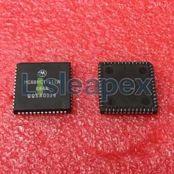
![MC68HC11E1FN]()
Constructed using CMOS technology and housed in a PQCC52 plastic package
Brand: Motorola Mobility Llc Package/Case: PLCC-52
6,968 In Stock
Cargo cycle: 3~7 Days
The minimum order is 1
-
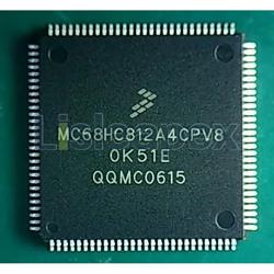
![MC68HC812A4CPV8]()
The MCHCPVis an efficient -bit microcontroller with a significant amount of program space ( RAM) and data storage ( EEPROM
Brand: Nxp Package/Case: LQFP-112
7,496 In Stock
Cargo cycle: 3~7 Days
The minimum order is 1
-
![DSP56002FC66]()
High-performance DSP chip featuring a floating-point unit
Brand: Nxp Package/Case: PQFP-132
6,271 In Stock
Cargo cycle: 3~7 Days
The minimum order is 1
-
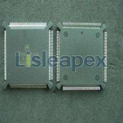
![XCF5206EFT40]()
PLASTIC RISC microprocessor with 32-Bit architecture running at 40MHz in PQFP160 package
Brand: Motorola Semiconductor Products Package/Case: QFP-16
3,123 In Stock
Cargo cycle: 3~7 Days
The minimum order is 1
-
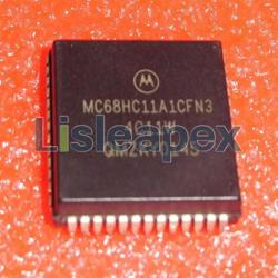
![MC68HC11A1CFN3]()
8-bit microcontroller with 256 RAM, A/D converter, and EEPROM
Brand: Nxp Package/Case: PLCC-52
4,058 In Stock
Cargo cycle: 3~7 Days
The minimum order is 1
-
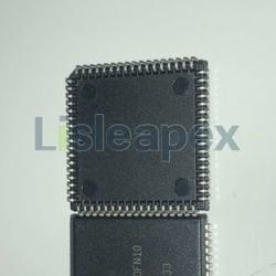
![MC68HC000FN10]()
The MC68HC000FN10 is a versatile 32-bit microprocessor with powerful capabilities
Brand: Freescale Semiconductor Package/Case: PLCC-68
6,620 In Stock
Cargo cycle: 3~7 Days
The minimum order is 1
-
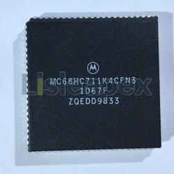
![MC68HC711K4CFN3]()
8-bit microcontroller with OTPROM, operating at a speed of 3MHz in a PQCC84 package
Brand: MOTOROLA Package/Case: PLCC84
4,143 In Stock
Cargo cycle: 3~7 Days
The minimum order is 1
-
![MC68EC000FN16]()
3,449 In Stock
Cargo cycle: 3~7 Days
The minimum order is 1
-
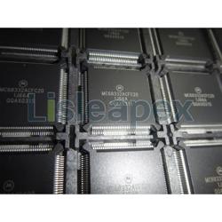
![MC68332ACFC20]()
7,389 In Stock
Cargo cycle: 3~7 Days
The minimum order is 1
-
![DSP56001ARC27]()
4,621 In Stock
Cargo cycle: 3~7 Days
The minimum order is 1
-
![MC68HC25FN]()
The MC68HC25FN is a versatile interface device manufactured by Motorola
Brand: MOTOROLA Package/Case: PLCC52
7,261 In Stock
Cargo cycle: 3~7 Days
The minimum order is 1
-
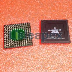
![MC68EC030RP40B]()
MC68EC030RP40B is a microprocessor chip manufactured by Motorola (now Freescale)
Brand: MOTOROLA Package/Case: PGA
5,713 In Stock
Cargo cycle: 3~7 Days
The minimum order is 1
-
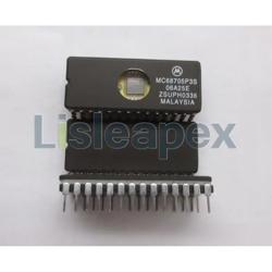
![MC68705P3S]()
MC68705P3S is a microcontroller chip developed by Motorola
Brand: MOTOROLA Package/Case: DIP-28
4,973 In Stock
Cargo cycle: 3~7 Days
The minimum order is 1
-
![XC68HC58FN]()
4,180 In Stock
Cargo cycle: 3~7 Days
The minimum order is 1
-
![MC68HC000FN20]()
3,804 In Stock
Cargo cycle: 3~7 Days
The minimum order is 1
-
![MC68HC000FN12]()
The MC68HC000FN12 is a powerful 16-bit microprocessor unit (MPU) designed for a wide range of applications
Brand: Freescale Semiconductor Package/Case: PLCC-68
6,061 In Stock
Cargo cycle: 3~7 Days
The minimum order is 1