Congratulations On Your Successful Submission
 Submission Failure
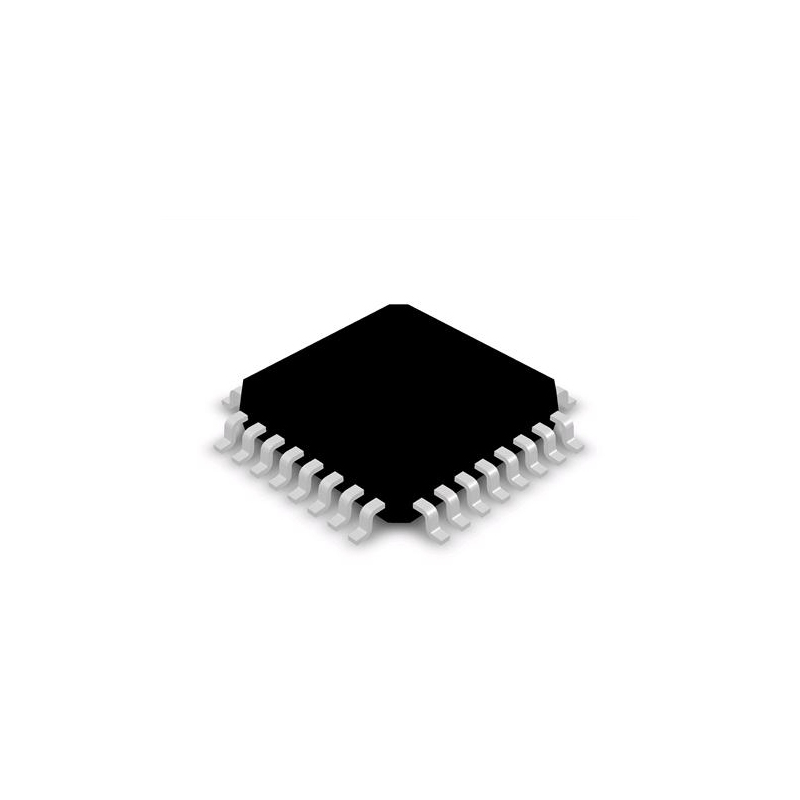
H5TQ1G63BFR-H9C
FPBGA-96 technology
H5TQ1G63BFR-H9C
FPBGA-96 technology
-
Manufacturer Part # : H5TQ1G63BFR-H9C
-
Package/Case: FBGA-96
-
Brand: SKHYNIX
-
Product Categories : Application Specific Clock/Timing
Quality Assurance
Quality Assurance
All parts procured from our supply chain network undergo a rigorous incoming inspection process. This meticulous inspection ensures that the parts received by our customers are authentic and meet the required standards. Additionally, we maintain detailed records of these inspections to ensure transparency and traceability throughout the supply chain.


Certification
We have successfully obtained various certification standards and have established our own professional testing laboratory. This ensures that every product we supply to our customers meets the highest quality standards. We adhere to strict testing protocols to maintain the consistency and accuracy of our products. To ensure that our products are original and genuine, we also collaborate with reputable third-party testing facilities to conduct rigorous quality testing. Our commitment to quality extends to meeting industry, legal, regulatory, and ISO 9001:2015 requirements.
Shipping & Payment
Shipping & Payment
About Shipping
We generally ship orders within a few business days through reliable shipping carriers such as FedEx, SF, UPS, or DHL. We also have support for other shipping methods. If you would like to inquire about specific shipping details or costs, please don't hesitate to reach out to us.


About Payment
We accept various payment methods, including VISA, MasterCard, UnionPay, Western Union, PayPal, and other channels.
If you have a specific payment method in mind or would like to inquire about rates and other details, please feel free to contact us.

WireTransfer

Paypal

CreditCard

WesternUnion

MoneyGram
Service & Packaging
Service & Packaging
About After Sales Service
All Parts Extended Quality Guarantee
Initiate the application within 90 days from the shipment date.
Confirm the return or exchange with our staff.
Maintain the goods in their original condition as received.
Lastly, please note that the eligibility for return or exchange of goods is subject to an assessment of the actual condition of the returned items. We will evaluate the received goods before finalizing the return or exchange process. If you have any inquiries or require further assistance regarding returns or exchanges, please don't hesitate to contact us at [email protected]
About packaging
Regarding packaging, our products are carefully packed in anti-static bags to provide ESD anti-static protection. The outer packaging is durable with secure closure. We support various packaging methods such as Tape and Reel, Cut Tape, Tube, or Tray.
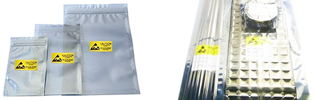
Example

Tape and Reel

Cut Tape

Tube or Tray
H5TQ1G63BFR-H9C DataSheet

Current price plan is under preparation. Please contact our customer service team for the latest pricing information. Thank you for your understanding and support!
Details
The H5TQ2G43CFR-xxC, H5TQ2G83CFR-xxC are a 2,147,483,648-bit CMOS Double Data Rate III (DDR3) Synchronous DRAM, ideally suited for the main memory applications which requires large memory density and high bandwidth. SK hynix 2Gb DDR3 SDRAMs offer fully synchronous operations referenced to both rising and falling edges of the clock. While all addresses and control inputs are latched on the rising edges of the CK (falling edges of the CK), Data, Data strobes and Write data masks inputs are sampled on both rising and falling edges of it. The data paths are internally pipelined and 8-bit prefetched to achieve very high bandwidth.FEATURES• VDD=VDDQ=1.5V +/- 0.075V• Fully differential clock inputs (CK, CK) operation• Differential Data Strobe (DQS, DQS)• On chip DLL align DQ, DQS and DQS transition with CK transition• DM masks write data-in at the both rising and falling edges of the data strobe• All addresses and control inputs except data, data strobes and data masks latched on the rising edges of the clock• Programmable CAS latency 5, 6, 7, 8, 9, 10, 11, 12, 13 and 14 supported• Programmable additive latency 0, CL-1, and CL-2 supported• Programmable CAS Write latency (CWL) = 5, 6, 7, 8, 9, 10• Programmable burst length 4/8 with both nibble sequential and interleave mode• BL switch on the fly• 8banks• Average Refresh Cycle (Tcase of0 oC~ 95oC) - 7.8 µs at 0oC ~ 85 oC - 3.9 µs at 85oC ~ 95 oC• JEDEC standard 78ball FBGA(x4/x8)• Driver strength selected by EMRS• Dynamic On Die Termination supported• Asynchronous RESET pin supported• ZQ calibration supported• TDQS (Termination Data Strobe) supported (x8 only)• Write Levelization supported• 8 bit pre-fetch• This product in compliance with the RoHS directive.
Key Features
- VDD=VDDQ=1.5V +/- 0.075V
- Fully differential clock inputs (CK, CK) operation
- Differential Data Strobe (DQS, DQS)
- On chip DLL align DQ, DQS and DQS transition with CK
- transition
- DM masks write data-in at the both rising and falling
- edges of the data strobe
- All addresses and control inputs except data,
- data strobes and data masks latched on the
- rising edges of the clock
- Programmable CAS latency 5, 6, 7, 8, 9, 10, 11, 12, 13
- and 14 supported
- Programmable additive latency 0, CL-1, and CL-2
- supported
- Programmable CAS Write latency (CWL) = 5, 6, 7, 8, 9, 10
- Programmable burst length 4/8 with both nibble
- sequential and interleave mode
- BL switch on the fly
- 8banks
- Average Refresh Cycle (Tcase of0 oC~ 95oC)
- - 7.8 µs at 0oC ~ 85 oC
- - 3.9 µs at 85oC ~ 95 oC
- JEDEC standard 78ball FBGA(x4/x8)
- Driver strength selected by EMRS
- Dynamic On Die Termination supported
- Asynchronous RESET pin supported
- ZQ calibration supported
- TDQS (Termination Data Strobe) supported (x8 only)
- Write Levelization supported
- 8 bit pre-fetch
- This product in compliance with the RoHS directive.
Specifications
The followings are basic parameters of the part selected concerning the characteristics of the part and categories it belongs to.
| Rohs Code | Yes | Part Life Cycle Code | Obsolete |
| Part Package Code | BGA | Pin Count ! | 96 |
| Reach Compliance Code | ECCN Code | EAR99 | |
| HTS Code ! | 8542.32.00.32 | Access Mode ! | MULTI BANK PAGE BURST |
| Access Time-Max | 20 ns | Additional Feature ! | AUTO/SELF REFRESH |
| Clock Frequency-Max (fCLK) | 667 MHz | I/O Type | COMMON |
| Interleaved Burst Length | 4,8 | JESD-30 Code | R-PBGA-B96 |
| JESD-609 Code | e1 | Length | 13 mm |
| Memory Density | 1073741824 bit | Memory IC Type | DDR3 DRAM |
| Memory Width | 16 | Number of Functions | 1 |
| Number of Ports ! | 1 | Number of Terminals | 96 |
| Number of Words | 67108864 words | Number of Words Code | 64000000 |
| Operating Mode ! | SYNCHRONOUS | Operating Temperature-Max | 85 °C |
| Operating Temperature-Min | Organization | 64MX16 | |
| Output Characteristics | 3-STATE | Package Body Material | PLASTIC/EPOXY |
| Package Code | TFBGA | Package Equivalence Code | BGA96,9X16,32 |
| Package Shape | RECTANGULAR | Package Style | GRID ARRAY, THIN PROFILE, FINE PITCH |
| Peak Reflow Temperature (Cel) | 260 | Power Supplies ! | 1.5 V |
| Qualification Status ! | Not Qualified | Refresh Cycles | 8192 |
| Seated Height-Max | 1.2 mm | Self Refresh | YES |
| Sequential Burst Length | 4,8 | Standby Current-Max | 0.01 A |
| Supply Current-Max | 0.26 mA | Supply Voltage-Max (Vsup) | 1.575 V |
| Supply Voltage-Min (Vsup) | 1.425 V | Supply Voltage-Nom (Vsup) | 1.5 V |
| Surface Mount ! | YES | Technology | CMOS |
| Temperature Grade ! | OTHER | Terminal Finish | Tin/Silver/Copper (Sn96.5Ag3.0Cu0.5) |
| Terminal Form ! | BALL | Terminal Pitch ! | 0.8 mm |
| Terminal Position | BOTTOM | Time@Peak Reflow Temperature-Max (s) | 20 |
| Width | 7.5 mm |
Specification Comparison
Datasheet PDF
Datasheets record the features, absolute maximum ratings, applications and more of the device, which benefit a lot as an overall guide to the specific application of the part.
Recommend Parts
-
![MPC93H52AC]()
Precise clock management solution for modern system-on-chip designs up to 240MHz
Brand: Renesas Electronics Corporation Package/Case: 32-LQFP
7,970 In Stock
Cargo cycle: 3~7 Days
The minimum order is 1
-
![MPC93H51AC]()
Precise frequency synthesis for accurate timing and synchronizatio
Brand: Renesas Package/Case: 32-LQFP
3,559 In Stock
Cargo cycle: 3~7 Days
The minimum order is 1
-
![H5TQ2G83EFR-PBC]()
3,303 In Stock
Cargo cycle: 3~7 Days
The minimum order is 1
-
![H5TC2G63GFR-PBA]()
Halon-free and RoHS compliant for eco-friendly designs
Brand: Sk Hynix Package/Case: FBGA-96
7,580 In Stock
Cargo cycle: 3~7 Days
The minimum order is 1
-
![DSC612PA1A-01H5]()
Accurate timing solutions for diverse industrie
Brand: Microchip Technology Package/Case: 6-VFLGA
4,925 In Stock
Cargo cycle: 3~7 Days
The minimum order is 1
-
![DSC612PA1A-01H5T]()
High-performance crystal oscillator for precise timing
Brand: Microchip Technology Package/Case: 6-VFLGA
3,362 In Stock
Cargo cycle: 3~7 Days
The minimum order is 1
-
![DSC612RA1A-01H5T]()
Robust frequency generation for precise timekeeping
Brand: Microchip Technology Package/Case: 6-VFLGA
5,556 In Stock
Cargo cycle: 3~7 Days
The minimum order is 1
-
![DSC612RA1A-01H5]()
Precision timekeeping solutions for demanding industries
Brand: Microchip Technology Package/Case: 6-VFLGA
2,200 In Stock
Cargo cycle: 3~7 Days
The minimum order is 1
-
![DSC612NA1A-01H5T]()
High-speed clock generation for precision timing application
Brand: Microchip Technology Package/Case: 6-VFLGA
7,728 In Stock
Cargo cycle: 3~7 Days
The minimum order is 1
-
![MPC93H51ACR2]()
The device has a clock frequency of Hz and uses PLL technolog
Brand: Renesas Electronics Corporation Package/Case: 32-LQFP
2,200 In Stock
Cargo cycle: 3~7 Days
The minimum order is 1
-
![8535AGI-31LF]()
Detailed product description: 8535AGI-31LF - Clock Buffer 1:4 for LVCMOS-to-3.3V LVPECL Fanout
Brand: Renesas Package/Case: TSSOP-20
7,143 In Stock
Cargo cycle: 3~7 Days
The minimum order is 1
-
![SY89297UMG]()
Dual Channel Delay Line with 5ps Step Delay
Brand: Microchip Technology Package/Case: QFN-24
5,645 In Stock
Cargo cycle: 3~7 Days
The minimum order is 1
-
![AD9516-3BCPZ]()
Wide range of operating frequencies and flexible output options
Brand: Analog Devices Package/Case: CP-64-4
5,070 In Stock
Cargo cycle: 3~7 Days
The minimum order is 1
-
![SY100EL34ZG]()
SY100EL34ZG
$7.389 Clock Generators & Support Products 3.3V /2, /4. /8 Clock Generation Chip
Brand: Microchip Technology Package/Case: SOIC-16
9,073 In Stock
Cargo cycle: 3~7 Days
The minimum order is 1
-
![SY87700VZC]()
8,933 In Stock
Cargo cycle: 3~7 Days
The minimum order is 1
-
![HT1381]()
HT1381
$0.412 Real-time Clocks (RTC) with single-line protocol in SOIC-8 package
Brand: Holtek Semicon Package/Case: SOIC-8
2,046 In Stock
Cargo cycle: 3~7 Days
The minimum order is 1