Congratulations On Your Successful Submission
 Submission Failure
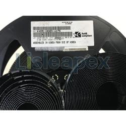
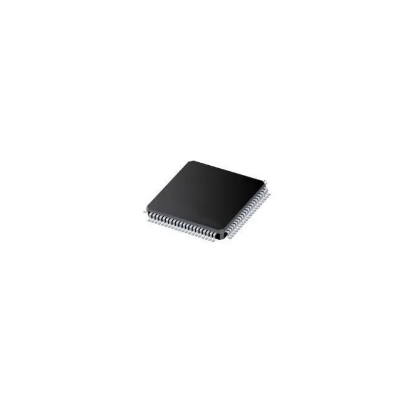
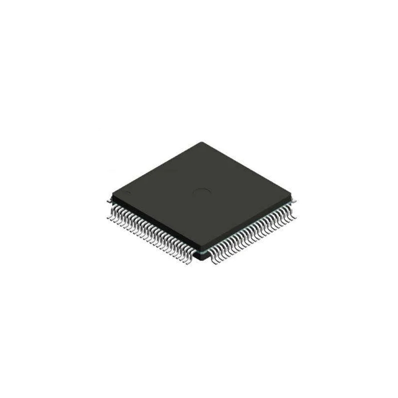
K4D263238F-QC50
Fast data transfer DDR DRAM module for high-performance application
K4D263238F-QC50
Fast data transfer DDR DRAM module for high-performance application
Quality Assurance
Quality Assurance
All parts procured from our supply chain network undergo a rigorous incoming inspection process. This meticulous inspection ensures that the parts received by our customers are authentic and meet the required standards. Additionally, we maintain detailed records of these inspections to ensure transparency and traceability throughout the supply chain.


Certification
We have successfully obtained various certification standards and have established our own professional testing laboratory. This ensures that every product we supply to our customers meets the highest quality standards. We adhere to strict testing protocols to maintain the consistency and accuracy of our products. To ensure that our products are original and genuine, we also collaborate with reputable third-party testing facilities to conduct rigorous quality testing. Our commitment to quality extends to meeting industry, legal, regulatory, and ISO 9001:2015 requirements.
Shipping & Payment
Shipping & Payment
About Shipping
We generally ship orders within a few business days through reliable shipping carriers such as FedEx, SF, UPS, or DHL. We also have support for other shipping methods. If you would like to inquire about specific shipping details or costs, please don't hesitate to reach out to us.


About Payment
We accept various payment methods, including VISA, MasterCard, UnionPay, Western Union, PayPal, and other channels.
If you have a specific payment method in mind or would like to inquire about rates and other details, please feel free to contact us.

WireTransfer

Paypal

CreditCard

WesternUnion

MoneyGram
Service & Packaging
Service & Packaging
About After Sales Service
All Parts Extended Quality Guarantee
Initiate the application within 90 days from the shipment date.
Confirm the return or exchange with our staff.
Maintain the goods in their original condition as received.
Lastly, please note that the eligibility for return or exchange of goods is subject to an assessment of the actual condition of the returned items. We will evaluate the received goods before finalizing the return or exchange process. If you have any inquiries or require further assistance regarding returns or exchanges, please don't hesitate to contact us at [email protected]
About packaging
Regarding packaging, our products are carefully packed in anti-static bags to provide ESD anti-static protection. The outer packaging is durable with secure closure. We support various packaging methods such as Tape and Reel, Cut Tape, Tube, or Tray.
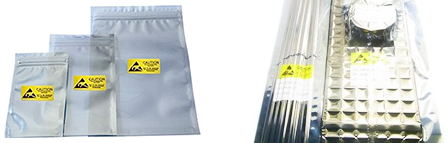
Example

Tape and Reel

Cut Tape

Tube or Tray
K4D263238F-QC50 DataSheet

Current price plan is under preparation. Please contact our customer service team for the latest pricing information. Thank you for your understanding and support!
Details
GENERAL DESCRIPTIONFOR 1M x 32Bit x 4 Bank DDR SDRAMThe K4D263238F is 134,217,728 bits of hyper synchronous data rate Dynamic RAM organized as 4 x 1,048,576 words by 32 bits, fabricated with SAMSUNG′s high performance CMOS technology. Synchronous features with Data Strobe allow extremely high performance up to 2.0GB/s/chip. I/O transactions are possible on both edges of the clock cycle. Range of operating frequencies, programmable burst length and programmable latencies allow the device to be useful for a variety of high performance memory system applications.FEATURES• 2.5V ± 5% power supply for device operation• 2.5V ± 5% power supply for I/O interface• SSTL_2 compatible inputs/outputs• 4 banks operation• MRS cycle with address key programs -. Read latency 3 (clock) -. Burst length (2, 4, 8 and Full page) -. Burst type (sequential & interleave)• Full page burst length for sequential burst type only• Start address of the full page burst should be even• All inputs except data & DM are sampled at the positive going edge of the system clock• Differential clock input• No Write Interrupted by Read function• Data I/O transactions on both edges of Data strobe• DLL aligns DQ and DQS transitions with Clock transition• Edge aligned data & data strobe output• Center aligned data & data strobe input• DM for write masking only• Auto & Self refresh• 32ms refresh period (4K cycle)• 100pin TQFP package• Maximum clock frequency up to 250MHz• Maximum data rate up to 500Mbps/pin
Key Features
- 2.5V ± 5% power supply for device operation
- 2.5V ± 5% power supply for I/O interface
- SSTL_2 compatible inputs/outputs
- 4 banks operation
- MRS cycle with address key programs
- -. Read latency 3 (clock)
- -. Burst length (2, 4, 8 and Full page)
- -. Burst type (sequential & interleave)
- Full page burst length for sequential burst type only
- Start address of the full page burst should be even
- All inputs except data & DM are sampled at the positive going edge of the system clock
- Differential clock input
- No Write Interrupted by Read function
- Data I/O transactions on both edges of Data strobe
- DLL aligns DQ and DQS transitions with Clock transition
- Edge aligned data & data strobe output
- Center aligned data & data strobe input
- DM for write masking only
- Auto & Self refresh
- 32ms refresh period (4K cycle)
- 100pin TQFP package
- Maximum clock frequency up to 250MHz
- Maximum data rate up to 500Mbps/pin
Specifications
The followings are basic parameters of the part selected concerning the characteristics of the part and categories it belongs to.
| Rohs Code | No | Part Life Cycle Code | Obsolete |
| Part Package Code | QFP | Pin Count ! | 100 |
| Reach Compliance Code | ECCN Code | EAR99 | |
| HTS Code ! | 8542.32.00.02 | Access Mode ! | FOUR BANK PAGE BURST |
| Access Time-Max | 0.7 ns | Additional Feature ! | AUTO/SELF REFRESH |
| Clock Frequency-Max (fCLK) | 200 MHz | I/O Type | COMMON |
| Interleaved Burst Length | 2,4,8 | JESD-30 Code | R-PQFP-G100 |
| JESD-609 Code | e0 | Length | 20 mm |
| Memory Density | 134217728 bit | Memory IC Type | DDR1 DRAM |
| Memory Width | 32 | Number of Functions | 1 |
| Number of Ports ! | 1 | Number of Terminals | 100 |
| Number of Words | 4194304 words | Number of Words Code | 4000000 |
| Operating Mode ! | SYNCHRONOUS | Operating Temperature-Max | 65 °C |
| Operating Temperature-Min | Organization | 4MX32 | |
| Output Characteristics | 3-STATE | Package Body Material | PLASTIC/EPOXY |
| Package Code | TQFP | Package Equivalence Code | TQFP100,.7X.9,25 |
| Package Shape | RECTANGULAR | Package Style | FLATPACK, THIN PROFILE |
| Power Supplies ! | 2.5 V | Qualification Status ! | Not Qualified |
| Refresh Cycles | 4096 | Seated Height-Max | 1.2 mm |
| Self Refresh | YES | Sequential Burst Length | 2,4,8,FP |
| Supply Voltage-Max (Vsup) | 2.625 V | Supply Voltage-Min (Vsup) | 2.375 V |
| Supply Voltage-Nom (Vsup) | 2.5 V | Surface Mount ! | YES |
| Technology | CMOS | Temperature Grade ! | COMMERCIAL |
| Terminal Finish | TIN LEAD | Terminal Form ! | GULL WING |
| Terminal Pitch ! | 0.65 mm | Terminal Position | QUAD |
| Width | 14 mm |
Datasheet PDF
Datasheets record the features, absolute maximum ratings, applications and more of the device, which benefit a lot as an overall guide to the specific application of the part.
FAQs
What is K4D263238F-QC50?
The K4D263238F-QC50 is a high-speed CMOS dynamic random-access memory (DRAM) module designed by Samsung. It offers fast and reliable data storage and retrieval capabilities, making it suitable for high-performance computing, servers, and networking applications.
How Does K4D263238F-QC50 Work?
The K4D263238F-QC50 works by storing and accessing data in a dynamic random-access fashion. It utilizes a matrix of capacitors to store charge representing binary data, which needs to be periodically refreshed to maintain data integrity. The module supports high-speed data transfer rates for efficient operation in demanding applications.
How Many Pins does K4D263238F-QC50 have and What are the Functions of the Pinout Configuration?
The K4D263238F-QC50 is typically found in a standard DDR SDRAM (Double Data Rate Synchronous Dynamic Random-Access Memory) form factor with 184 pins. The pinout configuration includes:
- Data Pins: For bi-directional data transfer between the module and the memory controller.
- Address Pins: For specifying the memory location to read from or write to.
- Control Pins: For managing data transfer operations and timing signals.
- Power and Ground Pins: For supplying power and ensuring proper grounding.
- Clock Pin: For synchronizing data transfers within the module.
What are the Pros and Cons of K4D263238F-QC50?
Pros:
- High Speed: Offers fast data transfer rates for rapid access to stored information.
- Reliability: Provides stable and reliable performance under demanding conditions.
- High Capacity: Offers significant memory storage capacity for processing large datasets.
- Compatibility: Designed to be compatible with standard DDR SDRAM interfaces.
- Efficiency: Supports efficient data transfer and processing for enhanced system performance.
Cons:
- Power Consumption: High-speed DRAM modules like the K4D263238F-QC50 may consume more power under heavy loads.
- Cost: Higher speed and capacity often come at a higher cost compared to lower-end memory modules.
- Complexity: Requires careful configuration and management to ensure optimal performance in the system.
Are There Any Equivalents/Alternatives to K4D263238F-QC50 for Recommendation?
- The MT47H64M16HR-25E:H from Micron Technology is a comparable high-speed DDR SDRAM module.
- Alternative options to the K4D263238F-QC50 include the H5TC4G63AFR-PBA from SK Hynix and the M471A2K43CB1-CRC from Samsung.
Recommend Parts
-
![K4S511632D-UC75]()
Distributor of electronic components based in France since 1988
Brand: Samsung Semiconductor Package/Case: TSOP-54
3,042 In Stock
Cargo cycle: 3~7 Days
The minimum order is 1
-
![K4D261638K-LC40]()
8MX16 GDDR1 DRAM module featuring a latency of 0.6ns, built on CMOS architecture, and encased in a PDSO66 package
Brand: SAMSUNG Package/Case: TSOP-66
7,893 In Stock
Cargo cycle: 3~7 Days
The minimum order is 1
-
![M393A8K40B21-CTC]()
M393A8K40B21-CTC
$24.491 This DRAM module offers a massive 64Gbyte of memory, making it ideal for use in 288RDIMM setups
Brand: SAMSUNG Package/Case: BGA
6,212 In Stock
Cargo cycle: 3~7 Days
The minimum order is 1
-
![M393A8K40B21-CRB]()
M393A8K40B21-CRB
$24.852 64GB DDR4 SDRAM memory module with 288 pins
Brand: SAMSUNG Package/Case: BGA
3,733 In Stock
Cargo cycle: 3~7 Days
The minimum order is 1
-
![M393A2K43CB1-CRC]()
M393A2K43CB1-CRC
$4.742 288-pin RDIMM DDR4 SDRAM 16Gbyte DRAM Module
Brand: SAMSUNG Package/Case: BGA
5,785 In Stock
Cargo cycle: 3~7 Days
The minimum order is 1
-
![K524G2GACB-A050]()
FBGA-137 type of DDR DRAM sorted by product code K524G2GACB-A050
Brand: SAMSUNG Package/Case: BGA
5,666 In Stock
Cargo cycle: 3~7 Days
The minimum order is 1
-
![HY57V161610DTC-7]()
Synchronous DRAM module with 1MX16 capacity, operating at 6ns speed, utilizing CMOS technology in a PDSO50 package measuring 0
Brand: SAMSUNG Package/Case: TSOP-50
4,122 In Stock
Cargo cycle: 3~7 Days
The minimum order is 1
-
![M393A1G40EB1-CRC]()
5,657 In Stock
Cargo cycle: 3~7 Days
The minimum order is 1
-
![M391A1G43EB1-CPB]()
6,256 In Stock
Cargo cycle: 3~7 Days
The minimum order is 1
-
![M393A1G40EB2-CTD]()
M393A1G40EB2-CTD
$9.065 RDIMM module designed for increased performance and reliability
Brand: SAMSUNG Package/Case: BGA
5,099 In Stock
Cargo cycle: 3~7 Days
The minimum order is 1
-
![M393A1G43EB1-CTD]()
6,958 In Stock
Cargo cycle: 3~7 Days
The minimum order is 1
-
![M393A1G40EB1-CPB]()
M393A1G40EB1-CPB
$6.562 Enhance your system's performance with this high-capacity M393A1G40EB1-CPB DDR4 SDRAM 8GB module."
Brand: SAMSUNG Package/Case: BGA
3,385 In Stock
Cargo cycle: 3~7 Days
The minimum order is 1
-
![M393B1G73EB0-YK0]()
4,629 In Stock
Cargo cycle: 3~7 Days
The minimum order is 1